Posts

sequential (105) No realistic serial circuit
Image
  https://wodewangzhishime.blogspot.com/2024/02/blog-post.html . Ref:  https://wodewangzhishime.blogspot.com/2024/02/blog-post.html . . . Me: Have a look .  https://wodewangzhishime.blogspot.com/2021/10/httpswodewangzhishime_90.html . . Hawaii fire which claim 130 people's lives. John:OK. Me: In reality, is there any serial circuit? John: Look at the above picture. Point A and B are parallel cirucit. I guess, point C is serial cirucit. John: You're wrong. Point C is a parallel circuit too.

sequential (104) smoothing capacitor

Image
  https://wodewangzhishime.blogspot.com/2023/12/blog-post_14.html   . Ref:  https://wodewangzhishime.blogspot.com/2023/12/blog-post_14.html . . . Me: There're 4 pictures above. . We mention the 1st picture. There is a full wave rectifier. . .When the smoothing capacitor discharge, the gap between the Up and Down cycle is filled. . Consequently, the wave-form of the direct current become smooth. . John: OK. . Me: Now, we look at the 2nd picture. . Case 1. high frequency  <--- The curve is very smooth. . The discharge of the smoothing capacitor can easily fill the gap. . Case 2. middle frequency <--- The curve isn't smooth. . The discharge of the smoothing capacitor can hardly fill the gap. . Case 3. low frequency <--- The curve can't continue. . . The direct current is broken. . The discharge of the smoothing capacitor can't fill the gap. . John: Now, we look at the 2nd picture. . . 1) In direct current, if the frequency is high, the discharge of the smoothing

sequential (103) R/W

Image
  https://wodewangzhishime.blogspot.com/2023/12/blog-post_43.html . Ref:  https://wodewangzhishime.blogspot.com/2023/12/blog-post_43.html  . . . The process is  1) register -> 2) Cache -> 3) Modulator -> 4) register. John: Inside the cache, there is a field called R/W status. .  Me: This field decide whether the field of value is read-only or read and write. . After the Xor gate checking, if the checking is correct, it will send a signal of 0 to the field of value. . The signal of 0 mean "opening the field of value" .

sequential (102) left shift

Image
https://wodewangzhishime.blogspot.com/2023/12/blog-post_13.html . Ref:  https://wodewangzhishime.blogspot.com/2023/12/blog-post_13.html  . . . . 1) The field of value is at the right-side most. 2) The field of value is right-shift unilateral. . John: Here comes a question. . If register 1 is master and register 2 is slave, what happen?? Me: I use the first picture as an example. Register 1 will create a cross over to swap the direction of the flow of the current. . Consequently, left-shift is available. .In reality, left-shift doesn't exist. John: In this case, the field of value will be affected. Me: No, because, the resistance of left shift is higher than the resistance of output. . . Me: I use the second picture as an example. . If the cross-over just cover the field of value. And, it doesn' cover the field of object, the field of value can not left-shift to the field of ojbect. . John: Both picture one and picture two work. 

sequential (101) delay circuit e

Image
  https://wodewangzhishime.blogspot.com/2023/12/blog-post_12.html . Ref:  https://wodewangzhishime.blogspot.com/2023/12/blog-post_12.html . . . Me: The upper picture use the inverters to delay the circuit. . However, the lower picture use the JK-Flip Flop to delay the circuit.

Sequential (100) delay circuit d

Image
https://wodewangzhishime.blogspot.com/2023/12/sequential-99.html . Ref :  https://wodewangzhishime.blogspot.com/2023/12/sequential-99.html .  . . Me: This article ( https://wodewangzhishime.blogspot.com/2023/12/blog-post_11.html ) mention that if I input 3-2-1-4, it stack overflow. Becuase 3-2 are too close to each other. .  . John: It is the problem of frequency. Me: Yes, . . Look at the 1st picture of this article. . It is an RJ45 circuit. .  This circuit use a capacitor and an inductor to form a filter. John: What's the filter for?? Me: For filtering signal. . . It let the signal within the boundary of frequency pass through. John: That mean, it let 3-2 enter the ground. Me: Yes,

sequential (99) mov object value

Image
https://wodewangzhishime.blogspot.com/2023/12/blog-post_11.html . . Ref: https://wodewangzhishime.blogspot.com/2023/12/blog-post_11.html   . . . . . Me: The following 4 articles mention how fields work in RAM. . They are very important. . Why ?? I answer you later. . Maybe,you can read them first. 1)  https://wodewangzhishime.blogspot.com/2021/11/httpswodewangzhishime_96.html 2)  https://kamchihau.blogspot.com/2022/10/httpskamchihau_17.html?m=1 3)  https://wodewangzhishime.blogspot.com/2022/06/satellite-for-loop.html 4)  https://kamchihau.blogspot.com/2022/11/httpskamchihau.html . Me: We deep inside the theme of today. . There're 6 fields inside a register. . They're the fields of Subject, Role, interrupt status, value's type, object and Value.  The field of Value is at the last position. Why??  Because, the field of Value is left shift forbiden. John: The fields of Subject,Role,interrupt,value's type and object are left/right shift bilateral.  Only, the field of value

sequential (98) delay circuit c

Image
https://wodewangzhishime.blogspot.com/2023/12/sequential-94-cross.html . Ref:  https://wodewangzhishime.blogspot.com/2023/08/is-that-due-to-wish-to-teach-americas.html . . . Me: https://wodewangzhishime.blogspot.com/2023/12/sequential-94-cross.html  . .This article mention that if you put too many inverters, the circuit delay too much. . Consequently, stack overflow occur. . Today, we give one more example in which the cirucit doesn't put too many inverters, however, stack overflow sitll occur. . I'm gonna input 3-2-1-4.   3-2 comply with the combination of NPN-PNP. . Look at the above picture. . There're 2 inverters only. . However, 3-2 both comply with the combination of NPN-PNP. . Consequently, stack overflow occur. . John: Because, 3-2 are closed to each other. . The frequency is too high. Me: In this case, stack overflow occur. . .

sequential (94) delay circuit b

Image
  https://wodewangzhishime.blogspot.com/2023/12/blog-post_2.html . Ref:  https://wodewangzhishime.blogspot.com/2023/12/blog-post_2.html  .  . . Me: You may consult it . . https://wodewangzhishime.blogspot.com/2023/12/blog-post_2.html .  Inverter is to delay the flow of current.  Normally, we put a pair of inverter. . In a single Up cylce, I input 3-2-1-4, indeed, only "3" can be input. . Why ?? Because, only "3" comply with the combination of NPN-PNP. . If you put too many inverters, the consequency is that not only "3" comply with the combination of NPN-PNP, but, "2" also comply with the combination of NPN-PNP. . Consequently, stack overflow occur.

sequential (93) delay circuit

Image
https://wodewangzhishime.blogspot.com/2023/12/sequential-92-smoothing-capacitor.html . Ref:  https://wodewangzhishime.blogspot.com/2023/12/sequential-92-smoothing-capacitor.html   . . . . . 1) About stack overflow, 2) Look at the 1st and 2nd pictures. . Note: The inverter delay the fow of current. The speed of the flow of current of line one is slower than the speed of the flow of current of line two. . 3) When the combination is npn-pnp, the up cycle is at the falling edge.  . 4) Look at the 3rd picture.  . John: When you input 3-2-1-4 to the gate of R1 during one up cycle, indeed, only 3 has the combination of NPN and PNP. .   And then , 2-1-4 are discarded. 3. npn pnp 2.  npn npn (discarded) 1.  npn npn (discarded) 4.  pnp npn (discarded) . John: Look at the last picture. . It is a RJ45 circuit. . .During an Up cycle, there're 3-2-1-4. . Me: Indeed, Port A only input with 3. . .And then, 2-1-4 are discarded. . Why ?? . John: Because, only "3" comply with the combinatio

sequential (92) - flip flop (3) - unstable

Image
  https://wodewangzhishime.blogspot.com/2023/12/blog-post.html . Ref:  https://wodewangzhishime.blogspot.com/2023/12/blog-post.html   . . John: Before we start, you may read this article first. <  https://kamchihau.blogspot.com/2024/07/sequential-109.html >. Me: OK. . John: This article  < https://wodewangzhishime.blogspot.com/2023/12/blog-post.html >  mention about a stable flip flop. You may read it first.   Me: OK. . John: Now, we start this article. Me: OK. John: At the above picture. There is an Up cycle on the clock line. This up cycle cover R0(0), R0(1), R0(2), R0(3). However, . R0(0)-> stable. R0(1)-> Unstable. R0(2)-> stable. R0(3)-> stable. . John: When R0(1) is unstable, R0(1) become a gap. Me: Then, what does gap mean? John: You may read this article. < https://wodewangzhishime.blogspot.com/2022/04/httpswodewangzhishime_23.html >. It is the meaning of "Gap".

sequential (91) - Flip flops (1) stable

Image
  https://wodewangzhishime.blogspot.com/2023/12/sequential-90-enabling-line.html . Ref:  https://wodewangzhishime.blogspot.com/2023/12/sequential-90-enabling-line.html . . . John: The above picture is a circuit of flip flop. I guess you know that . . When set and reset is 1-0 -> 1 0-1 -> 0 0-0 -> remain the same.  1-1 -> toggle or illegal.  . John: Do you see an Up cycle on the clock line? Me: Yes,. John: This Up cycle is stable.

sequential (90) stack overflow

Image
  https://wodewangzhishime.blogspot.com/2023/11/httpswodewangzhishime_29.html . Ref: https://wodewangzhishime.blogspot.com/2023/11/httpswodewangzhishime_29.html . . . Me: Here, we mention stack overflow. . You may read this article first.  https://wodewangzhishime.blogspot.com/2023/11/httpswodewangzhishime.html  . . I assume I have a 4 bits counter. . Originally, the 4 bits counter is 1-1-1-1. . if (4 bits counter = 0-0-0-0) { Mov object, value. } else { pending(); } . . John: During one Up cycle, if I input 0-0-0-0 to R1, what happen?? . Me: The result is always 0-1-1-1. . You can never achieve 0-0-0-0. . . John: So, how do I achieve 0-0-0-0?? . input 0 to R1 clear (or down cycle) input 0 to R1 clear (or down cycle) input 0 to R1 clear (or down cycle) input 0 to R1 clear (or down cycle)

sequential (89) - Stack Overflow

Image
  https://wodewangzhishime.blogspot.com/2023/11/httpswodewangzhishime.html . Ref:  https://wodewangzhishime.blogspot.com/2023/11/httpswodewangzhishime.html . . Me: I mention stack overflow in this article. . You can have a look at this article first.  https://wodewangzhishime.blogspot.com/2023/11/httpswodewangzhishime.html .  . Look at the first picture. If you input 3-1-4-2-4-1-3, the output is 3-3-3-3-3-3-3-3. You must 3-(input down cycle)1-(input down cycle)4-(input down cycle)2-(input down cycle)4-(input down cycle)1-(input down cycle)3 . Or. . You can 3-(power source, down cycle)1-(power source ,down cycle)4-(power source ,down cycle)2-(power source ,down cycle)4-(power source ,down cycle)1-(power source ,down cycle)3

sequential (88) - latch vs modulator

Image
https://wodewangzhishime.blogspot.com/2023/11/ref-httpswodewangzhishime.html . Ref: https://wodewangzhishime.blogspot.com/2023/11/ref-httpswodewangzhishime.html .  . . Those pictures are the difference between a latch and a modulator. . 1) The first picture is a latch. . During an Up cycle, I input 3-1-4-2-4-1-3. . The output remain 3-3-3-3-3-3-3. . Why ?? Because, it is a latch. . The output depends on the feedback. . If I wanna a 3-1-4-2-4-1-3, what should I do?? You should 3-(down cycle)1-(down cycle)4-(down cycle)2-(down cycle)4-(down cycle)1-(down cycle)3 . 2) The second picture is a modulator. . If I input 3-1-4-2-4-1-3, the output is 3-1-4-2-4-1-3. . Why ?? Because, the output is independent from the feeback. . 3) The third pictue is clear. . . . If there is a feedback, it is a latch. . If there is no feedback, it is a modulator.

sequential (87) RJ45 (Port A and Port B)

Image
https://wodewangzhishime.blogspot.com/2023/08/2001-4-airplanes-were-hacked.html?m=1 . Ref: https://wodewangzhishime.blogspot.com/2021/09/httpswodewangzhishime_11.html . . . . . . . John: Look at the first picture. Ther're 2 way of connection of RJ45. Both ways are OK. Let me explain the 2nd picture. Me: OK. John: When Port A is being input, Port B is with the status of outputing. Me: OK. . John: Look at the 3rd picture. When Port B is being input, Port A is with the status of outputing.

sequential (75) a RJ45 carrier wave (1)

Image
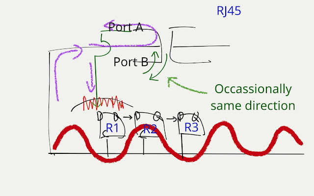
https://wodewangzhishime.blogspot.com/2023/08/is-that-due-to-wish-to-teach-americas.html . Ref:  https://wodewangzhishime.blogspot.com/2021/11/httpswodewangzhishime_83.html . . John: This article ( https://wodewangzhishime.blogspot.com/2022/03/httpswodewangzhishime_7.html ) mention about the direction of current flow of RJ45. Me: OK. John: Now, we look at the 3rd picture. The direction of current flow of the secondary coil must be opposite to the direction of the current flow of the primary coil. Me: Correct. If we don't do that, the current flow of the primary coil will stop. . John: Now, I change the story a little. Me: OK. . John: The direction of the current flow of the secondary is occassionally opposite to the direction of the current flow of the primary coil. Me: Occassionally? John: Yes,. Me: Then, a carrier wave will be formed. John: Now, we look at the 2nd picture. Me: OK. . If the direction of the current flow the Port B is occassionally same as the direction of the curr

sequential (97) Engine

Image
https://wodewangzhishime.blogspot.com/2023/08/blog-post.html . Ref:  https://wodewangzhishime.blogspot.com/2021/09/accompany-journalists.html  . . . . . At the above picture,  there is a cigarete lighter on the left hand side, and, a 2 stroke engine on the right hand side, . A cigarete lighter is same as a 2 stroke engine.  It need 1) a spark plug, 2) Oxygen, 3) Carbon hydrogen. . It is chemistry. . . . John: If the intaker  of cigarete-lighter is overheat, it explode. . . Same thing, if the intaker  of the 2 stroke engine is overheat, it explode as well. . . Me: I agree with you . .However, the intaker is working normally. .  Tell me . . .Why is the intaker  suddenly overheat ?? . John: The reason is here. . Have a look. .  https://wodewangzhishime.blogspot.com/2021/10/httpswodewangzhishime_0.html . . . . 1) An airplane of Russia explode.  https://en.m.wikipedia.org/wiki/2004_Russian_aircraft_bombings . .

sequential (74) RJ45 carrier wave (2)

Image
  https://wodewangzhishime.blogspot.com/2023/07/blog-post_31.html . . Ref:  https://kamchihau.blogspot.com/2023/08/blog-post.html   . . . John: Before we start, you may read this article ( https://wodewangzhishime.blogspot.com/2023/08/2001-4-airplanes-were-hacked.html ). . Me: OK. John: If the direction of current flow of port B is "occassionally" same as that of port A, there will be carrier wave formed. . Me: OK. John: Look at the picture above. Those carrier wave will affect the data input of Port A. Me: Those carrier wave also affect the Clock line. Consequently, register R1, 2, 3 become unstable.

sequential (72) Frequently used cache

Image
  https://wodewangzhishime.blogspot.com/2023/07/me-look-at-this-article.html . Ref: https://wodewangzhishime.blogspot.com/2023/07/me-look-at-this-article.html . . Register 5 can't send anything to register 4 " directly ". .  Register 5 must send to the cache of R4 first. .  And then, the cache of R4 will send to the modulator.  .  Lastly, the modulator will send to Register 4. . John: There're the cache of R1,2,3,4,5. .Next to the cache of R1,2,3,4,5, there 're Xor gates which are used to compare and check. . If the signal from register 5 enter the loop-back line, does the signal of register 5 need to goes into the Xor gate of R1,2,3,4,5 for comparing and checking ?? Me: Indeed, the signal of register 5 need go through the xor gate of R1,2,3,4,5 . However, in reality, it doesn't need it. John: Why ?? Me: There're 3 Loop-back line. . They are L1 loop-back line, L2 loop-back line, L3 loop-back line. . Indeed, on the L1 loop-back line, only R4 has an Xor gate

sequential (71) RJ45 output triggering point

Image
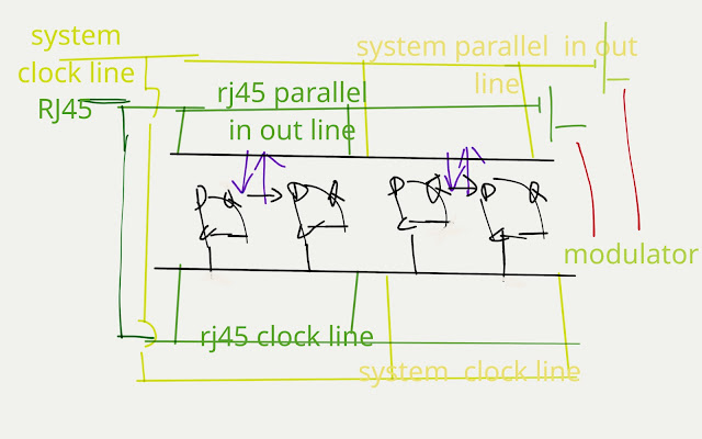
  https://wodewangzhishime.blogspot.com/2023/07/blog-post.html . Ref: https://wodewangzhishime.blogspot.com/2023/07/blog-post.html . . . John: The above picture is the process of output of RJ45. The first step is MOV Port C, value. Me: And then? . 1) The data input of R3 is from the data output of R2 (R2 right shift to R3) 2) The data input of R2 is from the data output of R1. (R1 right shift to R2) . John: Then, where is the data input of R1 from? Me: From the clock line. John: That mean, the data-input line of R1 is linked to the clock line. Me: Correct. When the clock line is up cyle, R1 is being triggered. We call that point as "Output triggering point". John: When Port A is triggered, R1 right shift to R2, R2 right shift to R3, etc. Me: Finally, R3 output. .

sequential (70) latch unlatched

Image
  https://wodewangzhishime.blogspot.com/2023/02/httpswodewangzhishime.html . Ref: https://wodewangzhishime.blogspot.com/2021/12/httpswodewangzhishime_28.html?m=1   . . . Me: The above picture is a transistor-latch . . This latch is formed by one PNP transistor and one NPN transistor. . T1,2 stand for transistor 1, 2. John: When we give a positive voltage to the gate of T1, T1 will be conducted forever. . We call that a latch. . Me: How can we let a latch unlatch ?? . VSS stand for source of power. . 1) Give a negative voltage to the gate of T1 or 2) Cut the VCC. . That mean , cut the source of power. . John: A latch is to temporarily latch the data in the memory, when the latch unlatch, the memory will lose forever.

sequential (19) Master-Slave

Image
https://wodewangzhishime.blogspot.com/2023/02/translate-selected-text.html . Ref: https://wodewangzhishime.blogspot.com/2023/02/if-ipaddress133133-nathon-road.html . . . . There're 5 conditions on which left or right shift doesn't work. . 1) The latch is being preset and clear. 2) The latch is feedbacking. 3) The latch is being level-trigger. 4) The flip flops is toggling. 5) The commutator is idle . . No up cycle. . No down cycle. Me: Now, we mention condition_3. . The D of master-regiser is being (level triggered). . Consequently, the master-register didn't left shift, nor did the master right shift. . John: Why ?? . Me: When it is right-shift, falling edge trigger. . When it is left-shift, rising edge trigger. . John: When it is level trigger, which side is the register shift?? . Me: No side . . The master-register just output the value to the output line, and then, the signal enter the cache and modulator. . Finally, the modulator send the signal to the slave register.

sequential (28) shift direction

Image
  https://wodewangzhishime.blogspot.com/2023/02/if-ipaddress133133-nathon-road.html Ref:  https://wodewangzhishime.blogspot.com/2022/06/httpswodewangzhishime_8.html . . . . Me: This picture is just my design. . In reality, it may not be like this. . If the current of the commuator is flowing to the right, and, the cycle is at up, only the NPN is saturated. . . Me: In this case, the output of Q can't left shift. . John: If output of Q left shift, the commutator must be at the down cycle, and the current must flow to the left hand side, and the PNP must be saturated. . .That mean, the PNP receive a signal of zero.